


Cynthia_HitechPCB_manufacturing Hitech Circuits PCB's Store
easyid.live/biz/cynthia-hitechpcb-manufacturing • Verified Store
Scan to open official EasyID digital store and view live catalog.
Share Cynthia_HitechPCB_manufacturing Hitech Circuits PCB's Store
Share this store link with your friends and customers
Cynthia_HitechPCB_manufacturing Hitech Circuits PCB's Store
Open Now • Open 24/7Verified Merchant
EasyID Certified Seller
Fast 24h Packing
Direct courier dispatch
Zero Escrow Direct
Direct merchant settlement
Store Listings (4)
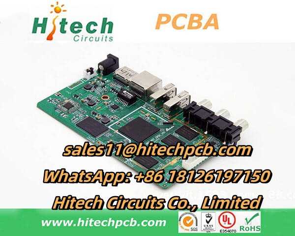
Briefly describe the basic process of PCBA patch processing
Briefly describe the basic process of PCBA patch processing <br> <br>The basic process of PCBA processing is to carry out SMT patch of components on the PCB board, DIP plug-in and realize welding. Here Hitech will briefly describe the basic process of PCBA processing for you. <br> <br>The PCBA processing process can be roughly divided into the following processes: SMT patch processing → DIP plug-in processing → PCBA testing → finished product assembly. <br> <br>1. SMT patch processing <br> <br>1). Solder paste stirring <br>The solder paste needs to be stirred before it can be used after it is taken out and thawed. <br> <br>2). Solder paste printing <br>The solder paste on the steel mesh is printed on the PCB pad by a scraper. <br> <br>3). SPI <br>SPI is the solder paste thickness detector. <br> <br>4). Mounting <br>The chip components are placed on the feeder, and the chip mounter head accurately mounts the components on the feeder on the PCB pad by identification. <br> <br>5). Reflow soldering <br>The mounted PCB board is reflowed to heat the solder paste into liquid and then cool and solidify to complete the welding process. <br> <br>6). AOI <br>AOI is automatic optical inspection, which detects the welding effect of PCB boards to eliminate bad PCB boards. <br> <br>7). Rework <br>Rework bad boards detected by AOI and manual inspection. <br> <br>2. DIP plug-in processing <br> <br>1). Plug-in <br>Insert the plug-in material on the PCB board. <br> <br>2). Wave soldering <br>The inserted board is soldered by wave soldering. <br> <br>3). Cutting the pins <br>The pins of the soldered board are generally too long and need to be cut. <br> <br>4). Post-welding processing <br>Use a soldering iron to manually solder the components. <br> <br>5). Washing the board <br>After wave soldering, the board will be dirty and needs to be cleaned with washing water and washing tank, or by machine. <br> <br>6). Quality inspection <br>Inspect the PCB board, unqualified products need to be repaired, and qualified products can enter the next process. <br> <br>3. PCBA testing <br> <br>According to different products and different customer requirements, different test methods are used to detect whether the PCBA products meet the PCBA processing requirements. <br> <br>4. Finished product assembly <br> <br>The PCBA products that have passed the test will be assembled into shells, and then tested. If the test is passed, it can be arranged for shipment. <br> <br>Hitech PCBA can provide you with high-quality SMT patch processing services, and also has rich PCBA processing experience. Hitech provide one-stop PCBA service for you. Hitech can also undertake DIP plug-in processing and PCB production, electronic circuit board manufacturing. <br> <br>If you have interest in our service, please feel freely contact Cynthia at sales11@hitechpcb.
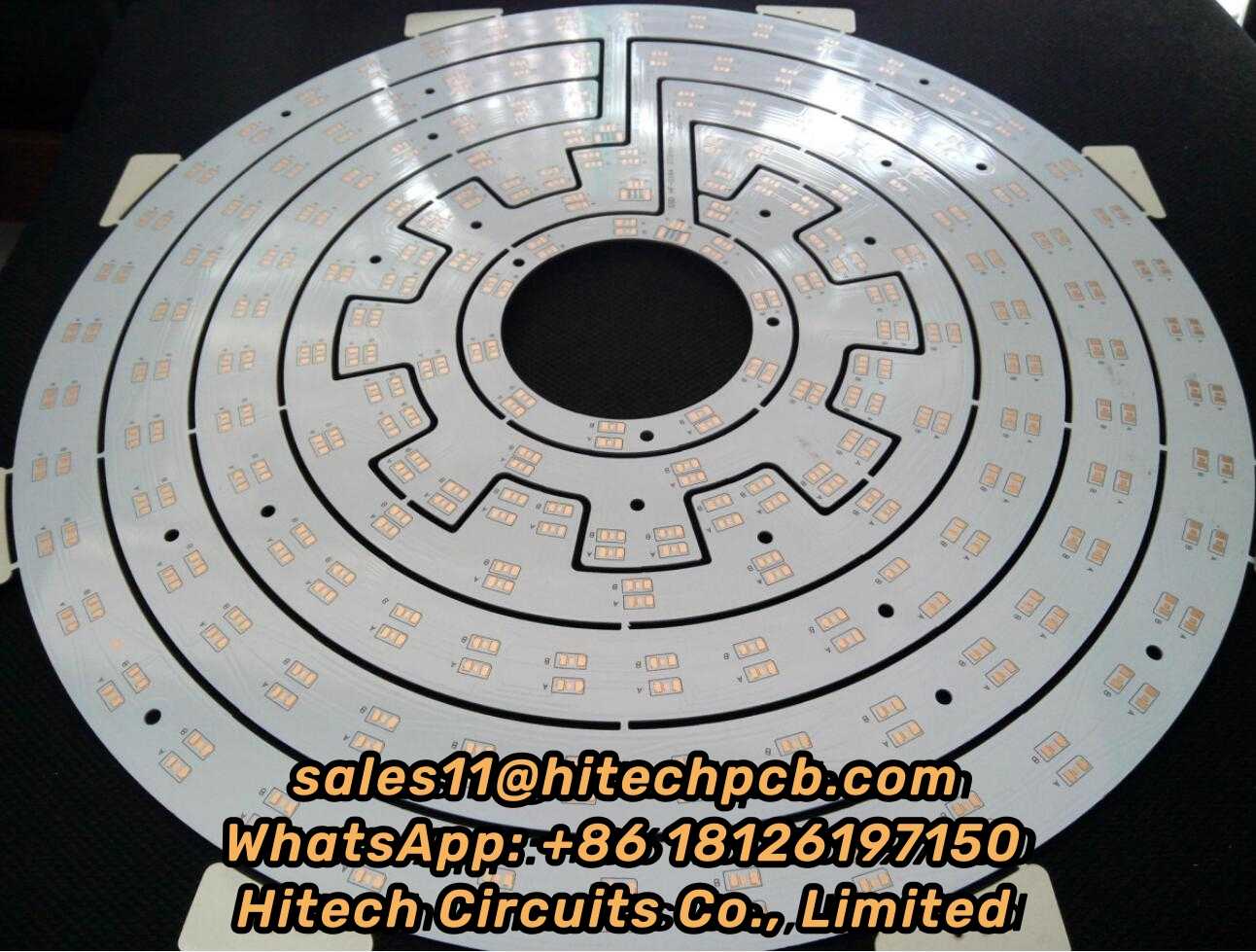
Different kinds of Aluminum PCBs
Different kinds of Aluminum PCBs <br> <br>Flexible Aluminum PCBs <br>One of the newest developments in IMS materials is flexible dielectrics. These materials feature a polyimide resin system with ceramic fillers which provides excellent electrical insulation, flexibility and of course thermal conductivity. When applied to a flexible aluminum material like 5754 or similar, the product can be formed to achieve a variety of shapes and angles which can eliminate costly fixtures, cables and connectors. Although these materials are flexible, they are intended to be bent into place and remain in place. They are not suited for applications that are intended to be flexed regularly. <br> <br>Hybrid Aluminum PCBs <br>In a ‘Hybrid’ IMS construction a “Sub-assembly” of a non-thermal material is processed independently and then bonded to the aluminum base with thermal materials. The most common construction is a 2-Layer or 4-Layer Sub-assembly made from conventional FR-4. Bonding this layer to an aluminum base with thermal dielectrics can help dissipate heat, improve rigidity and act as a shield. Other benefits include: <br>Less costly than a construction of all thermally conductive materials <br>Provides superior thermal performance over a standard FR-4 product <br>Can eliminate costly heat sinks and associated assembly steps <br>Can be used in RF applications where a surface layer of PTFE is desired for its’ loss characteristics. <br>Use of component windows in the aluminum to accommodate through-hole components. This allows connectors and cables to pass connections through the substrate while the solder fillet creates a seal without the need for special gaskets or other costly adapters. <br> <br>Multilayer Aluminum PCBs <br> Common in the high performance power supply market, multilayer IMS PCBs are made from multiple layers of thermally conductive dielectrics. These constructions have one or more layers of circuitry buried in the dielectric with blind vias acting as either thermal vias or signal vias. While more expensive and less efficient at transferring heat as a single layer designs, they provide a simple and effective solution for heat dissipation in more complex designs. <br> <br>Through-Hole Aluminum PCBs <br>In the most complex constructions a layer of aluminum can form a ‘Core’ of a multilayer thermal construction. The aluminum is pre-drilled and back-filled with dielectric prior to lamination. Thermal materials or sub-assemblies can be laminated to both sides of the aluminum using thermal bonding materials. Once laminated, the completed assembly is thru-drilled similar to a conventional multilayer PCB. The plated through holes pass through the clearances in the aluminum to maintain electrical insulation. Alternatively a Copper core can allow both direct electrical connections as well as with insulated through holes. <br> <br>If you want to know ceramic PCBs, please feel freely to contact Cynthia at [email protected]
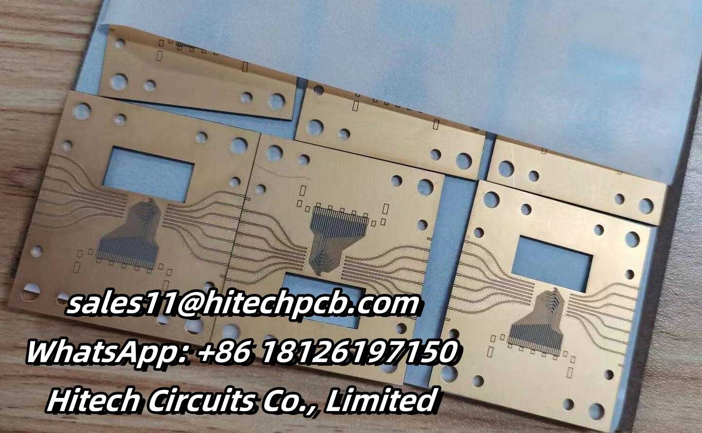
Why use ceramics for circuit boards?
Why use ceramics for circuit boards? <br> <br>Ceramic circuit boards are actually made of electronic ceramics material and can be made into various shapes. Among them, the ceramic circuit board has the most outstanding characteristics of high temperature resistance and high electrical insulation performance, and has the advantages of low dielectric constant and dielectric loss, high thermal conductivity, good chemical stability, and similar thermal expansion coefficient of the component, and Ceramic printed circuit boards are produced using LAM technology, a laser rapid activation metallization technology. Used in LED field, high power semiconductor module, semiconductor cooler, electronic heater, power control circuit, power mixing circuit, intelligent power component, high frequency switching power supply, solid state relay, automotive electronics, communication, aerospace and military electronics Component. <br> <br>Unlike traditional FR-4 (glass fiber) , ceramic materials have good high-frequency performance and electrical properties, and have high thermal conductivity, chemical stability and thermal stability. The ideal packaging material for a generation of large-scale integrated circuits and power electronics modules. <br> <br>Main advantages: <br> <br>1. Higher thermal conductivity <br> <br>2. be assembled in high density <br> <br>3. Good insulation <br> <br>4. The solder ability of the substrate is good and the use temperature is high <br> <br>5. More matching coefficient of thermal expansion <br> <br>6. Low frequency loss <br> <br>7. A harder, lower resistance metal film aluminum oxide ceramic circuit board <br> <br>8. Free of organic constituent, resistant to cosmic rays, high reliability in aerospace and long service life <br> <br>9. The copper layer does not contain an oxide layer and can be used for a long time in a reducing atmosphere. <br> <br>If you want to know ceramic PCBs, please feel freely to contact Cynthia at [email protected]
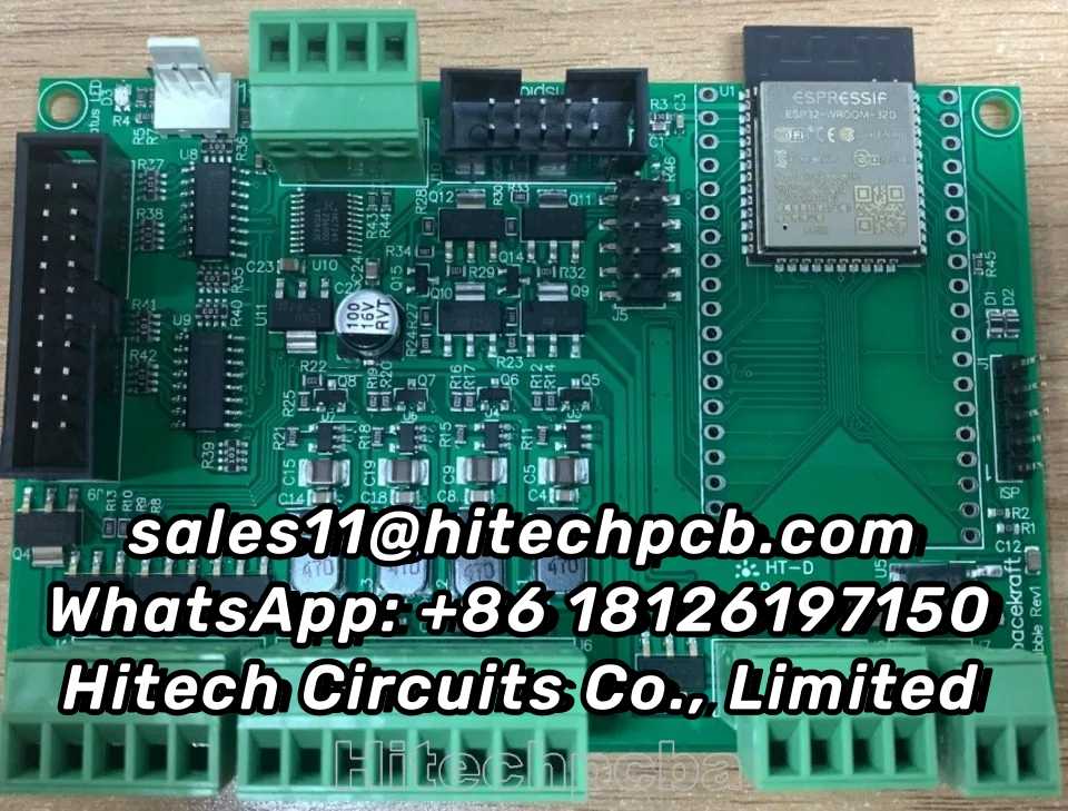
PCB Assembly Prototypes Manufacturer – Hitech Circuits Co., Limited
PCB Assembly Prototypes Manufacturer – Hitech Circuits Co., Limited <br> <br>What is a prototype PCB assembly? <br> <br> PCB prototyping is the experimentation pilot stage of the product which is to be mass produced at a later stage. This is more of an experiment which is done after the initial discussions and the design. This offers a pre-production analysis of the boards that are to be manufactured, reducing the possible number of errors in the PCB design. PCB prototypes help the manufacturer analyze the strengths as well as weak areas of their proposed circuit boards. Prototypes also serve as a reference point for future versions of the same product. At Hitechpcba, we handle PCB prototype assembly in quantities from one to hundred printed circuit boards. <br> <br> <br>We have acquired capabilities that enable us to serve our clients better. All these years, we have worked on many complex prototype PCB assembly projects, and we believe the following capabilities have helped us serve our clients better. <br> <br>Prototype PCB Assembly Services: We specialize in the following prototype printed circuit board assembly services. <br> <br>SMT: We can provide single-sided and double-sided surface mount PCB assemblies in different specifications. <br> <br>Plated Through Hole: We offer plated through hole assembly with selective soldering. <br> <br>Mixed Assemblies: We often work on projects involving mixed assemblies – through-hole and SMT and electromechanical assemblies. <br> <br>PCBA Testing: All the PCBA functional testing is performed in-house. Over the years, we have invested in various test fixtures and equipment, which helps us ensure the quality of PCBA. Currently, we provide the following types of PCBA testing services: <br> <br>Flying probe testing for PCB <br> <br>Functional testing including system and board-level testing <br> <br>General PCB Assembly Capabilities: Our general PCB assembly capabilities are not limited to these: <br> <br>RoHS, leaded or lead free, clean and no chemistries <br> <br>PCB components including various types of QFNs, BGAs, 0105, 0201, 0804, and press fit components in small quantities. <br> <br> <br>What are the benefits of a prototype PCB assembly? <br> <br>Prototype PCB assembly comes with several advantages. These benefits play a major role in the facilitation of your PCB manufacturing. Some of these benefits include: <br> <br> <br>Detection of Flaws Early <br> <br>With prototype PCB, you will easily detect whatever flaws are present during the product’s development stages. This will allow you to solve the issues thereby saving you some money if you had gone ahead to make the production having the flaws in them. <br> <br>If you go ahead to make changes during the production, there may be a need for more technicalities, and this may be expensive. <br> <br> <br>Testing of Each Component <br> <br>With a prototype, you will be able to test all your system’s elements individually before you go ahead to set it up. You should do this because it is important especially for very complex projects composed of several parts that are PCB based. <br> <br>When you validate each of these components, you will be able to identify those areas having issues that you should look into. This is the only way the project can function the right way. <br> <br> <br>Reduction in Total Costs <br> <br>Utilizing the prototype bare PCB for any of your projects could go a long way in reducing what you’ll have spent in total for the project. With prototyping, you will be able to notice those errors in your project and then make corrections before you start the real production. <br> <br>As soon as these flaws have been checked and rectified, then you may continue with the manufacturing of your Printed circuit boards in large quantities, thereby saving you unnecessary costs. <br> <br> <br>High-Quality PCBs <br> <br>Why prototyping your PCB is important is to help you test if your project will function effectively. When we talk of testing, it involves the identification of errors present and then rectifying and making corrections to them. <br> <br>Therefore, the eventual PCB after the prototyping will be of high quality that surely meets standards set internationally. <br> <br> <br>Less Turnaround Time <br> <br>With prototype PCB assembly, you will be able to reduce the total time used in producing your printed circuit board. While making use of prototype printed circuit boards, you’ll be able to see the errors and then make corrections before you start the actual production. <br> <br>Therefore, the eventual prototype will be free of defects. This implies that your PCBs will be produced quickly by your manufacturer. <br> <br> <br>What are the different types of prototype PCB assembly services you offer? <br> <br>With years of market presence and experience, we specializes in the following prototype PCB assembly services. <br> <br>Plated through-hole (PTH): We can provide the through-hole assembly with selective soldering. <br> <br>Surface mount technology (SMT): We offer single-sided as well as double-sided SMT board assemblies in varied specifications. <br> <br>Mixed Assemblies: Our experts often work on projects involving both PTH and SMT assemblies. <br> <br> <br>What are the types of testing Hitechpcba use for prototype PCB assembly? <br> <br>Automated Optical Inspection (AOI): This is performed before and after the soldering to identify the component placement, presence, and solder quality. <br> <br>X-ray Testing: In this type of testing, the operator relies on the X-ray images of the PCB to check the solder joints and lead-less components such as Quad Flat Packs and ball grid arrays, which are generally not visible to naked eyes. <br> <br>In-Circuit Testing (ICT): This method is used to detect manufacturing defects by testing the electrical properties in the SMT Assembly. <br> <br>These techniques help us ensure the reliability and accuracy of the circuit boards. In addition to this, it ensures a long operational life of equipment, minimal production losses, streamlined processes, and much more. <br> <br> <br>What are the capabilities Hitechpcba offer for prototype PCB assemblies? <br> <br>We specialize in offering IPC compliant, and quick turn PCB assemblies. We are very particular about our scheduled deliveries and timelines, and we deliver without compromising the quality. Our PCBA capabilities are not limited to these. Here are some capabilities we offer through prototype PCB assemblies. <br> <br>RoHS compliance <br> <br>Stringent testing procedures <br> <br>Device encapsulation <br> <br>Full turnkey, partial turnkey, and kitted/consigned services <br> <br>Assemblies using Surface Mount (SMT), Thru-hole, Mixed Technology (SMT/Thru-hole), Single and double-sided SMT/PTH, Large parts on both sides, BGA on both sides. <br> <br> <br>Do you perform a component analysis for prototype PCB assemblies? <br> <br>Yes, we check the quality and performance of components before mounting them on the circuit boards. This is because a malfunctioning component can affect the performance of the entire circuit board assembly and also pose risks. <br> <br> <br>What is your standard turnaround time for a prototype PCB assembly? <br> <br>Our turnaround time for standard applications is two weeks. This timeframe varies depending on the complexity of the applications. However, we are committed to offering quick turnaround times without compromising on quality, functionality, and accuracy, which offers our client a competitive advantage and reduced time to market. You can also request any emergency assistance or queries related to any type of PCB assembly. Our experts will assist you in all possible ways. <br> <br> <br>How is the cost of prototype PCB assembly estimated? <br> <br>PCBA costing varies based on the different factors, such as PCBA parts, type of materials to be used, order quantity, and much more. We can also offer quotes and customization options once you share the detailed requirement with us. <br> <br>We focus on quality and customer satisfaction over anything else. This has helped us build a long list of happy and satisfied customers. So, if you wish to partner with a manufacturer of prototype PCB assembly in China, then don’t hesitate to reach us. Our experts will assist you through all the phases of the prototype PCB assembly process. We look forward to making your experience with us better and memorable. <br> <br> <br>How to choose prototype pcb assembly manufacturer? <br> <br>Our pcb prototype assembly service includes the sourcing of components. This allows you to concentrate on what you do best: layout design. We have a dedicated sourcing staff that coordinates with multiple suppliers and distributors to purchase electronic parts as per client requirements, and our staff completes these purchasing particulars in a most efficient manner. We have advanced processes for optimal selection of packaging (cut tape, tube, bulk, etc.) to reduce the total cost. Furthermore, we are capable of cross-referencing parts and even locating hard-to-find and obsolete parts. Customers can be rest assured that when Hitech Circuits substitutes components that they are high quality: we only use the electronic component numbers and manufacturers specified in the BOM. We will not modify your original layout design. Part substitutions take place only with your permission. <br> <br>The final pcb prototype assembly service cost includes assembly labor charges, bare circuit board rates, and part costs. We understand the importance of prompt delivery. The sooner the components are sourced, the sooner we can begin circuit board fabrication. We thoroughly evaluate engineering inquiries and concerns related to the related parts with our clients before commencing circuit board assembly. The average time taken for pcb manufacturing assembly is about two weeks, which can be further reduced if there are no hard-to-locate components or documentation mistakes. <br> <br>We have specialized experts to deliver fast turnarounds for prototype circuit board assembly with surface-mount (SMT), through-hole (THT) and mixed-technology components. <br> <br>Anyone interested in electronics and electronic circuit boards needs to understand the various stages of developing and producing a printed circuit board. It can come in handy when you are seeking a top prototype smt assembly provider. The various production stages of printed circuit boards entail design, prototyping (prototype PCB development and rapid prototyping pcb assembly), and PCB high volume production. Different entities will always seek part of the whole production process depending on their electronic circuit board needs. <br> <br>However, this article seeks to help you understand everything about prototype PCB assembly, a fundamental aspect of the PCB production process. <br> <br>Rapid prototyping pcb assembly represents a fundamental phase of the printed circuit production process. It is also inferred as PCBA prototype assembly, SMT or surface-mount technology PCB prototype, PCB sample assembly, etc. From these alternative names, the meaning of prototype assembly regarding printed circuit boards becomes apparent. So what is assembly prototype? <br> <br>PCB prototype assembly service is a fast prototype printed circuit board assembly primarily used to test fresh or new electronic designs. Consequently, it assists with checking and ensuring quality assurance of the PCB. For instance, it verifies that no bug exists in the test PCB, updates the design, and finds bugs. In most instances, prototype assembly of an electronic project will require two or three iterations to ensure everything is perfect. <br> <br> <br>Why Choose Hitech Circuits PCB Assembly for Your Prototype PCB Assembly Projects? <br> <br>There are several PCB manufacturers specializing in prototype PCB assembly services. However, Hitech Circuits stands out owing to the following: <br> <br>1.Strong Supply Chain: Over the years, we have built strong supply chain relationships in the industry, which helps us fulfill the requirements of turnkey prototype assembly services easily. <br> <br>2.Fastest Turnaround Times: Our engineering expertise coupled with our understanding of industry requirements and a well-equipped facility enables us to assure the fastest turnaround times of 24-48 hours. <br> <br>3.Reliability: All the printed circuit boards that we produce are IPC compliant, which helps us assure reliability. <br> <br>4.Competitive Pricing and Quick Quote: Our supply chain relationships enable us to assure competitive prices. The cost of the PCB prototype assembly will be made available within 24-48 hours. <br> <br>For further details freely contact Cynthia at [email protected] <br>[a]https%3A%2F%2Fwww.hitechpcba.com%2Fpcb-assembly-manufacturer[/a]
About Cynthia_HitechPCB_manufacturing Hitech Circuits PCB's Store
No description provided.
0.0
Customer Reviews
See what others are saying about Cynthia_HitechPCB_manufacturing Hitech Circuits PCB's Store. We verify purchases to ensure reviews are genuine.
No reviews yet for this store.