



hh circuits's Store
easyid.live/biz/hhcircuits • Verified Store
Scan to open official EasyID digital store and view live catalog.
Share hh circuits's Store
Share this store link with your friends and customers
hh circuits's Store
Open Now • Open 24/7Verified Merchant
EasyID Certified Seller
Fast 24h Packing
Direct courier dispatch
Zero Escrow Direct
Direct merchant settlement
Store Listings (2)
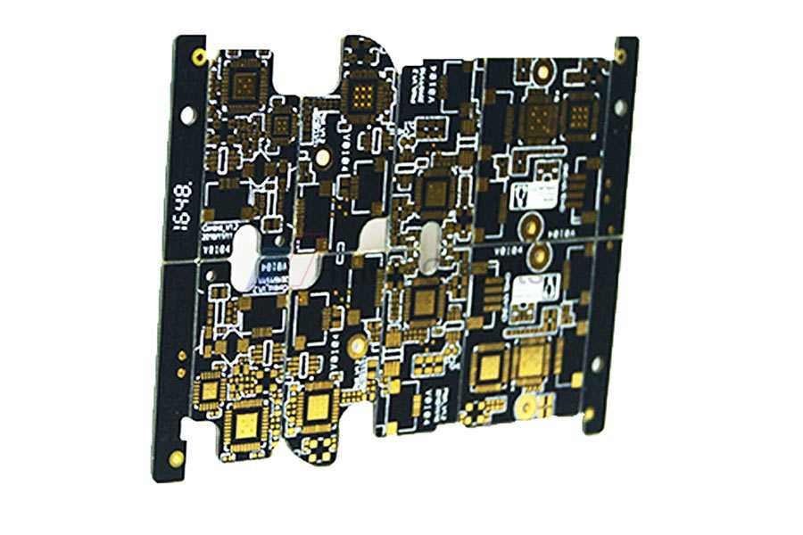
Heavy Copper PCB Manufacturer
Heavy Copper PCB, pcb fabrication up to 12oz, large current, pcb circuit fabrication base material is FR4/Teflon/Ceramic, pcb fabrication used in high-power power supply and motor circuits products. HUIHE CIRCUITS is one of the heavy copper PCB manufacturers, we have passed ISO9001/ISO13485/IATF16949/UL/RoHS/REACH certification.If you want to know more about thick copper pcb, heavy copper pcb, please contact HUIHE Circuits heavy copper pcb board manufacturer. <br> <br>Heavy Copper PCB List <br>2 Layer ENIG Heavy Copper PCB circuit manufacturer <br> <br>4 Layer ENIG Heavy Copper PCB <br> <br>6 Layer ENIG Heavy Copper PCB supplier <br> <br>6 Layer ENIG Heavy Copper PCB manufacturing <br> <br>6 Layer ENIG Heavy Copper PCB Fabrication Service <br> <br>6 Layer ENIG Heavy Copper PCB <br> <br>8 Layer ENIG Heavy Copper PCB <br> <br>8 Layer ENIG Impedance Control Heavy Copper PCB <br> <br>2 Layer ENIG Heavy Copper PCB <br> <br>The Heavy Copper PCB Plating Process Must Achieve The Following Aspects: <br>1. HUIHE Circuits heavy copper pcb manufacturer adds a certain value according to the area value calculated by the computer and the empirical constant accumulated in the actual production to ensure the integrity of the plating layer in the hole. <br>2. When the heavy copper PCB is electroplated for 5 minutes, take out the substrate and observe whether the copper layer on the surface and the inner wall of the hole is intact. It is better that all the holes have a metallic luster. <br>3. A certain distance must be maintained between the substrate and the substrate. <br>4. When the heavy copper PCB reaches the required electroplating time, a certain amount of current must be maintained during the removal of the substrate to ensure that the surface of the substrate and the hole will not be blackened or darkened. <br>5. HUIHE Circuits heavy copper pcb manufacturer according to the mechanical processing floppy disk for trial processing, the first part pre-inspection is carried out, and all the workpieces are processed after meeting the technological requirements. <br>Heavy Copper PCB Manufacturer Quality Control <br>1. HUIHE Circuits heavy copper PCB manufacturer Strictly implements the first article inspection system to ensure that the product size meets the design requirements. <br>2. According to the raw materials of different types of pcb boards, reasonably select the milling process parameters. <br>3. When fixing the position of the circuit board, HUIHE Circuits heavy copper PCB manufacturer carefully clamps it so as not to damage the solder layer and solder mask on the surface of the circuit board. <br>4. To ensure the consistency of the substrate dimensions, HUIHE Circuits heavy copper PCB manufacturer must be strictly controlled the position accuracy . <br>5. When disassembling and assembling, HUIHE Circuits heavy copper PCB manufacturer pays special attention to the barrier layer of the substrate and pad paper to avoid damage to the coating layer on the surface of the circuit board. <br>Applications Of Heavy Copper PCB <br>Heavy copper PCBs shine in applications that demand high power and efficient heat management. Here are some key areas where they are widely used: <br> <br>Power Electronics: This is a major domain for heavy copper PCBs. They are ideal for power supplies, motor controllers, and other high-current devices. Their ability to handle large currents and dissipate heat effectively makes them perfect for these applications. <br>Industrial Automation: Industrial equipment often involves high-power motors, drives, and converters. Heavy copper PCBs ensure smooth operation by handling substantial currents and dissipating the generated heat. <br>Automotive Industry: Modern vehicles use increasingly complex electronic systems, including power converters and inverters. Heavy copper PCBs provide the necessary current capacity and thermal management for these applications. <br>Aerospace and Defense: These sectors demand reliable and high-performance electronics. Heavy copper PCBs meet these needs with their superior current handling and heat dissipation. <br>Other Applications: They can also be found in welding equipment, power distribution units, power line monitors, torque controls, overload relays, and protection relays. <br>Overall, anywhere you need a PCB to handle significant power and manage the resulting heat, heavy copper PCBs are a strong choice. <br>#heavy#copper#pcb#manufacturers <br>[a]https%3A%2F%2Fwww.hhcircuits.com%2Fheavy-copper-pcb[/a]
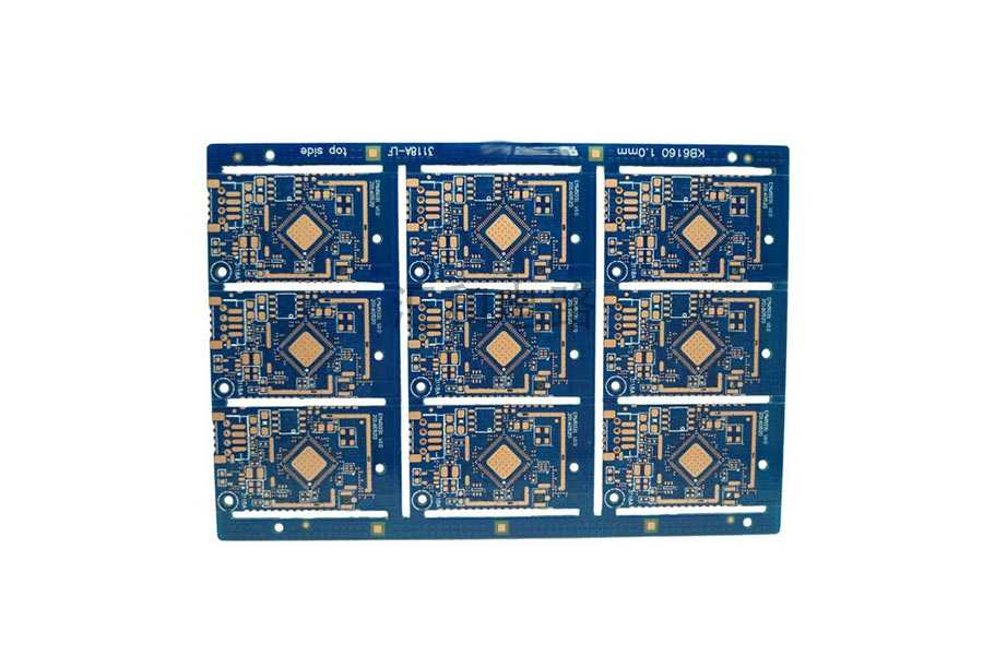
Half Hole & Through Hole Pcb
Through hole circuit board & half hole PCB, no copper burr residue or warpage in half hole, reduce connectors and save space, apply to Bluetooth module and Signal receiver products. HUIHE CIRCUITS PCB board with holes apply to Bluetooth module and Signal receiver products. Our PCB products have passed ISO9001/ISO13485/IATF16949/UL/RoHS/REACH certification. <br> <br>Half Hole & Through Hole PCB List <br>2 layer OSP impedance control half hole PCB <br>2 layer ENIG half hole PCB <br>4 layer ENIG impedance control half hole PCB electric circuit board <br>2 layer ENIG impedance control half hole PCB <br>8 layer ENIG half hole custom PCB <br>4 layer ENIG impedance control half hole fr4 PCB <br>4 layer ENIG impedance control half hole PCB <br>4 layer LF-HASL half hole PCB <br> <br>Production Process Of Metallized Half-Hole PCB <br>For the front inversion, to prevent the quality of the product and the need to make corrections in the later process, the production process of this type of board is processed according to the following process: a drilling (drilling, gong groove-plate surface plating-external Optical imaging-pattern plating-co-drying-half-hole processing-film stripping, etching, tin stripping-other processes-shape <br> <br>Main Points Of Metallized Half-Hole PCB Production <br>The specific metallized PCB half holes are processed in the following way: all metallized half-hole PCB holes must be drilled in the pattern after plating, and one hole at the intersection of the two ends of the half-hole should be drilled before etching. <br> <br>The engineering department formulates the MI process according to the process <br>The metal half-hole is the second-drilled half-hole drilled during the first drilling (or gong), after the image is plated, and before the etching. It is necessary to consider whether the copper will be exposed when the gong groove is shaped, and move the drilled half-hole into the unit. <br>he right hole is drilled first, and then the board is turned over (or mirrored) and the left hole is drilled to reduce the pulling of the copper of the inner hole of the half hole by the drill, resulting in the lack of copper of the hole. <br>The size of the drill nozzle for drilling the half hole depends on the spacing of the contour lines. <br>Draw the solder mask film, use the gong space as a stop point and open the window to increase 4mil treatment. <br>The Designer's Suggestion When Designing The Circuit <br>Change the distance from the edge line to the hole center. The general design is to place the hole center on the edge line and move the control center down. For example, the diameter of the hole is 1.4mm, the distance between the two holes is 2.54mm, and the board edge The distance between the line is 0.33mm from the center of the through hole, and the thickness of the plate is 0.6mm. The angle between the tangent to the cut point of the wall and the track of the milling cutter was 90 degrees before, but this time it is about 60 degrees. Because the board edge line is at a certain distance from the center of the through hole, the cutting angle of the milling cutter is changed, and the board thickness is extremely small, so the copper in the hole is not easily pulled out. The simultaneous improvement of small batch pcb design and production can greatly improve the production yield of PCB half-hole boards. <br> <br>As a pcb board maker, we will do our best to meet all the needs of customers. <br>#half#hole#pcb <br>[a]https%3A%2F%2Fwww.hhcircuits.com%2Fhalf-hole-through-hole-pcb[/a]
About hh circuits's Store
No description provided.
0.0
Customer Reviews
See what others are saying about hh circuits's Store. We verify purchases to ensure reviews are genuine.
No reviews yet for this store.